
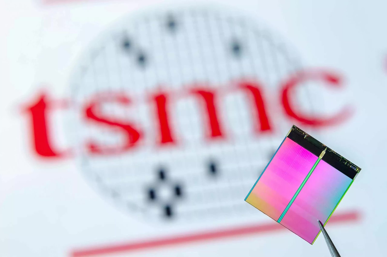
TSMC’s most advanced process node is moving faster than the company’s own schedule. The chipmaker has pulled pilot production of its A14 process, its 1.4-nanometer-class node, forward to the first quarter of 2027, earlier than originally planned, according to TrendForce and Global Sources.
The A14 node is the next step in the shrinking of the transistors that power everything from phones to AI accelerators. Moving it into early production sooner than expected gives TSMC’s customers a faster path to chips that are faster and draw less power than the current generation.
TSMC is pressing ahead on four factories for the 1.4-nanometer node, all targeted to begin production before 2030, according to the reports. The company has said the node will deliver a full step down in size along with gains in performance and efficiency.
The acceleration comes as TSMC spends at a pace that reflects its position at the center of the AI supply chain. Capital spending this quarter reached $15.59 billion, up 42 percent from the prior quarter, according to the reports, as the company adds capacity for both leading-edge manufacturing and the packaging that assembles finished AI chips.
A day before the A14 reports, Taiwan broke ground on a new advanced-packaging industrial park in the southern city of Kaohsiung, anchored by TSMC. Packaging has become the second bottleneck in the AI chip supply chain, and TSMC has been building capacity in Taiwan and abroad to keep it from constraining the chips themselves.
The two developments point in the same direction. Advanced process technology and advanced packaging are the two tightest links in the chain that feeds Nvidia, AMD and the other companies whose chips run AI systems, and TSMC is adding capacity in both at once.
TSMC’s lead in manufacturing has made it the company every major chip designer depends on. That dependence has deepened as AI systems have grown, because the most advanced accelerators are built on TSMC’s newest nodes and assembled with its most advanced packaging.
The A14 timeline has drawn attention because of how quickly TSMC is moving through generations. The company’s previous node, A16, is still ramping, and the decision to begin pilot production of its successor early suggests TSMC sees demand for even faster chips arriving sooner than it once expected.
Analysts said the acceleration is partly a response to competition and partly a reflection of customer pressure. Apple, Nvidia, AMD and others plan their roadmaps around TSMC’s nodes years in advance, and any delay in a new process ripples through their product plans.
TSMC has also been expanding beyond Taiwan. The company has built or planned fabs in the United States, Japan and Germany, a geographic diversification driven as much by customer demand and government subsidies as by the desire to spread risk.
The Kaohsiung packaging park is the latest piece of that expansion. Packaging capacity has been one of the few areas where TSMC’s customers have had to wait, and the new site is meant to relieve a constraint that has, at times, held back the chips themselves.
A14 follows A16, the node TSMC is now ramping for its most advanced customers. Moving to a new node on a faster cadence is a measure of the demand TSMC sees, and of the pressure from customers whose product cycles no longer tolerate the longer gaps between generations that were once routine.
TSMC manufactures the majority of the world’s most advanced chips, and its dominance has only grown as the cost of developing new process technology has climbed beyond the reach of all but a few companies. Intel and Samsung, its two would-be rivals, have both struggled to match TSMC’s pace and yields.
The company’s largest customers, Apple and Nvidia among them, design their silicon around TSMC’s roadmap years in advance. Apple has historically been first to adopt each new node for its phone processors, and the schedule TSMC now sets for A14 will shape when those products reach store shelves.
Packaging has become nearly as important as the process node itself. Modern AI chips stitch together multiple pieces of silicon, and the advanced packaging that connects them is a specialized capability few companies possess. TSMC’s push into Kaohsiung is aimed at a constraint that has, at times, delayed the chips themselves.
For TSMC’s rivals, the pace is hard to match. Intel and Samsung have struggled to keep their own advanced nodes on schedule, and every month TSMC moves a new process forward widens the distance between it and the companies trying to close the gap.
The company has not committed to a date for high-volume A14 production, and the reports describe pilot production, the first stage in which a new node makes working chips in small numbers. But the direction is clear: TSMC is pulling the next generation forward while spending to make sure nothing downstream holds it up.
For the AI economy, that is the relevant signal. The chips that will power the next wave of models and data centers are already being scheduled, and TSMC has decided they need to arrive sooner than planned.