
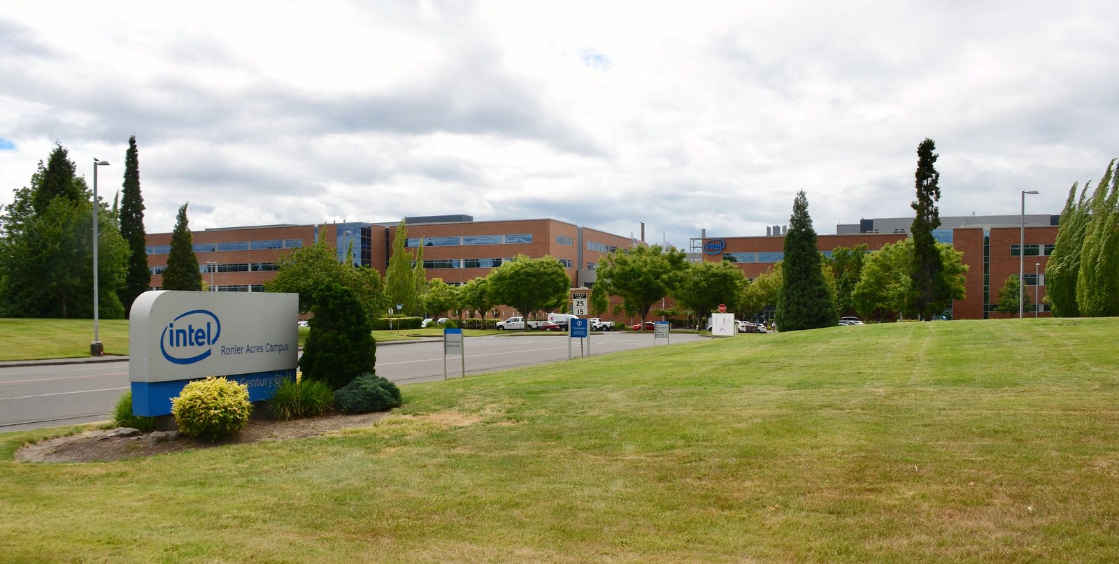
Intel and Applied Materials said they would expand a research partnership to jointly develop the process technology and materials behind the next generation of AI chips. The announcement, made on Oct. 8, is a bet that the hardest problems in making faster semiconductors can no longer be solved by any one company alone.
Under the arrangement, Intel will join a chip research lab that Applied Materials runs in Silicon Valley, a roughly $500 million facility where the equipment maker has already brought together a range of partners. Taiwan Semiconductor Manufacturing, Intel’s rival in contract chipmaking, sits in the same collaborative network, a sign of how unusual the grouping has become.
The two companies are responding to a problem that has reshaped the industry. As chips for artificial intelligence have grown larger and more complex, the bottlenecks have moved from raw design to the process of manufacturing them: how finely features are etched, how materials behave at the smallest scales, and how chips are stacked and packaged to squeeze out more performance.
Applied Materials makes the machines that build chips. Intel makes the chips. Binding the two together at the research stage shortens the distance between an idea about a new material and its use on a production line. It also means that a process change Intel wants for its next chip can be tested on Applied Materials’ equipment before either company commits to a full rollout.
The partnership carries particular weight for Intel, which has spent years trying to regain ground in advanced manufacturing after falling behind TSMC. Intel has staked a large part of its turnaround on building a foundry business that can win customers, and on regaining leadership in the most advanced process nodes. Working more closely with the top equipment maker is part of that effort.
For Applied Materials, the value runs the other way. Its fortunes rise and fall with the capital spending of the big chipmakers, and closer ties to a customer of Intel’s scale give it earlier visibility into what those customers will need next. The company has described its Silicon Valley lab as a place where the industry’s hardest problems can be attacked before they reach the factory floor.
Applied Materials occupies a central position in the supply chain. It is one of the world’s largest makers of semiconductor manufacturing equipment, and its tools sit inside fabs run by every major chipmaker. When it opens its research lab to a customer, the cooperation carries the weight of an industry standard.
The relationship is not symmetrical, and neither company pretends otherwise. Intel needs the process leadership that has slipped from its grasp, while Applied Materials needs a flagship customer willing to co-develop at the frontier. Each brings something the other lacks, which is what makes the pairing more than a courtesy call between two Silicon Valley neighbors.
The announcement stops short of a merger or a joint venture. It is a research collaboration, and the companies did not disclose its financial terms or its duration. What they disclosed is the direction: process technology and materials for AI chips, the area where the industry’s attention and its money are concentrated.
That focus reflects a broader change in the economics of chipmaking. For decades, the industry improved by shrinking transistors, a predictable march that lifted everyone. That path has become harder and more expensive, and the gains now come from a mix of new materials, new packaging techniques, and tighter integration between design and manufacturing.
Analysts said the pairing makes sense at a moment when the cost of a single leading-edge fab runs into the tens of billions of dollars and no single company can afford to master every step alone. Collaboration that once looked like a concession now looks like a necessity.
The alliance also carries a competitive signal. TSMC has long enjoyed the closest relationships with its equipment and materials suppliers, part of the ecosystem that keeps it ahead. Intel’s move into Applied Materials’ lab is, in part, an effort to build a similar set of ties.
The companies framed the work as addressing the specific demands of AI chips, which use more advanced materials and more sophisticated packaging than the processors of the past. Those chips consume enormous power and generate enormous heat, and squeezing more performance out of them requires changes to the very materials from which they are built.
Neither company suggested the collaboration would produce a chip on its own. The output of a research lab is knowledge, and the question is how fast that knowledge moves into products. The two companies are betting that by sitting at the same table, they can move it faster than either could alone, and faster than a customer waiting on the next generation of chips would otherwise allow.