Scott DeBoer opened the section of Micron’s technology briefing that analysts had come for with a sentence that was not on his slides. Asked when memory supply would finally catch up with demand, the company’s president and chief technology officer declined to name a date. “We do not see a period of time where memory is not going to be in short supply in the next two years,” he said.
That answer explains the roadmap he then walked through. Micron has spent the past three years selling scarce high-bandwidth memory into AI servers and watching the rest of its product line follow the same supply squeeze. The plan it laid out this week is less about any single part than about holding a cadence: a new DRAM node every eighteen months, a new NAND generation that skips a number, and a set of products aimed at data centers rather than the consumer market that once paid the bills.
The first piece is the 1-delta DRAM node, scheduled to ramp in the second half of 2027 with a bit density gain in the mid-twenties percent over 1-gamma. It will be manufactured in the United States, and it will underpin DDR6, LPDDR6, and the memory that goes into HBM5 and Micron’s stacked variants. 1-gamma, the company’s first node built with extreme ultraviolet lithography, is already in high-volume manufacturing, and Micron says it will be the highest-volume node in its history.
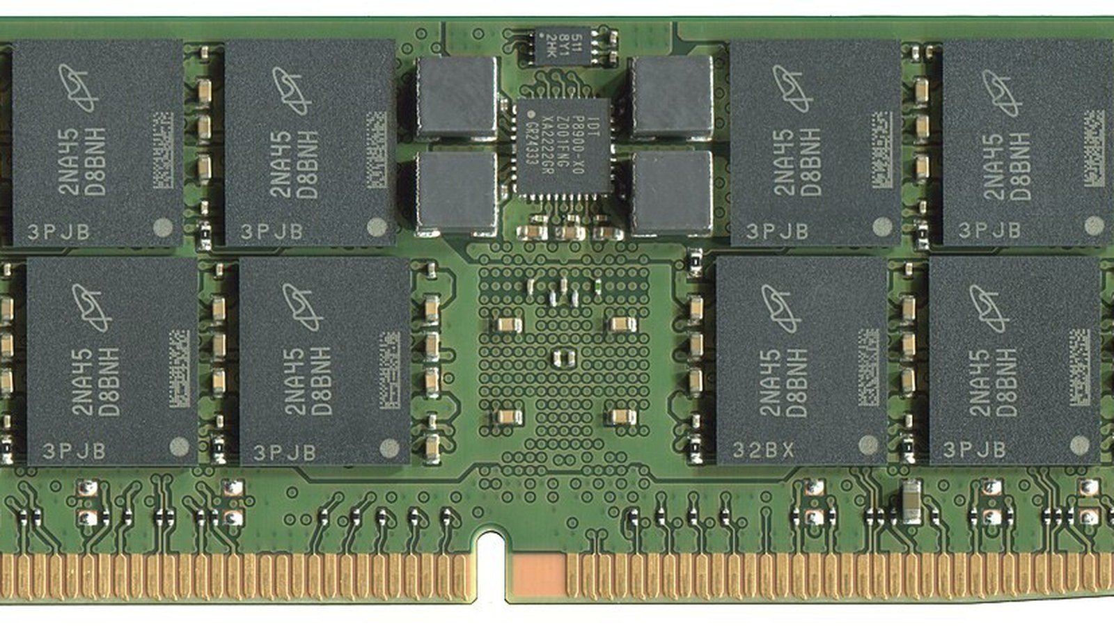
DDR6 is the part of the plan most likely to be misread. Its bandwidth is more than double DDR5’s, which sounds like the successor that will appear in desktop machines and laptops on a normal schedule. Micron is positioning it as server memory for AI data centers, sold on reliability and error correction rather than on the consumer upgrade cycle. The company also plans a 1-terabyte RDIMM module, a capacity that only makes sense in a machine running inference against a model too large to fit in cache. In September it demonstrated a 512-gigabyte DDR5 RDIMM running at 9,200 megatransfers per second, a sign of how much of the roadmap is already in silicon.
The NAND side of the briefing drew more attention because of what Micron chose not to build. The company is skipping its tenth generation entirely and going from G9 to G11, which will carry more than 400 layers and roughly double the bit density of the current part. G9, shipping now in products such as the Crucial P510, has 276 layers. G11 will also lift input-output speed by about half and cut the energy needed to move a bit by at least a quarter.
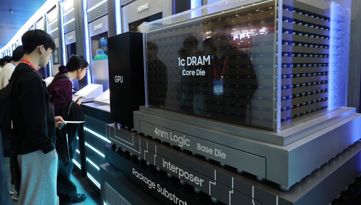
Skipping a generation is a statement about time. Each 3D NAND generation requires new deposition and etch tools, new test flows, and a customer qualification cycle that can run nine months. Collapsing two generations into one saves a full round of that overhead, at the cost of a harder engineering problem. Micron will build G11 with wafer-on-wafer bonding, gluing two wafers together so that the memory array and the logic beneath it are made on separate lines optimized for each. That is the same manufacturing idea the industry is using to stack DRAM, and G11 is effectively the proof that it works at production scale before Micron needs it for memory.
The architectural choice underneath all of this is the one analysts spent the most time on. Samsung, SK hynix, and China’s CXMT are all developing 4F-squared DRAM cells, which shrink the area per bit by redesigning the access transistor. Micron is not. It is extending its existing 6F-squared cell through 1-delta and several nodes beyond, then moving to wafer bonding at 1-epsilon and eventually to a true three-dimensional DRAM. Rivals are funding two transitions. Micron is funding one, on the argument that 4F-squared shrinks the transistor while the capacitor above it still sets the pitch, so the density gain is smaller than the geometry suggests.
It is a defensible bet and a risky one. If 4F-squared yields at advanced geometries, Micron will have given away a node of density to competitors who can then stack their own 3D designs on top of it. If it does not, Micron arrives at 3D DRAM with its capital and its supplier relationships pointed in one direction.
The commercial backdrop makes the schedule matter more than usual. HBM4 entered high-volume manufacturing in March, HBM4E is sampling and due to ramp in 2027, and Micron is now offering custom HBM designs co-developed with customers, work that requires a base die built on a foundry process rather than its own. Data center demand for off-chip memory is forecast to grow from about $97 billion this year to $260 billion by 2030, according to Futurum Group.
The company’s own claim is that AI-assisted engineering has halved the time from design to manufacturing, with an SSD controller reaching tape-out in half the usual span. That claim comes from flash programs rather than DRAM nodes, and the harder test is whether Micron can ramp 1-delta and G11 in the same six-month window without either slipping. The roadmap is credible. The calendar is the part still to be proven.