
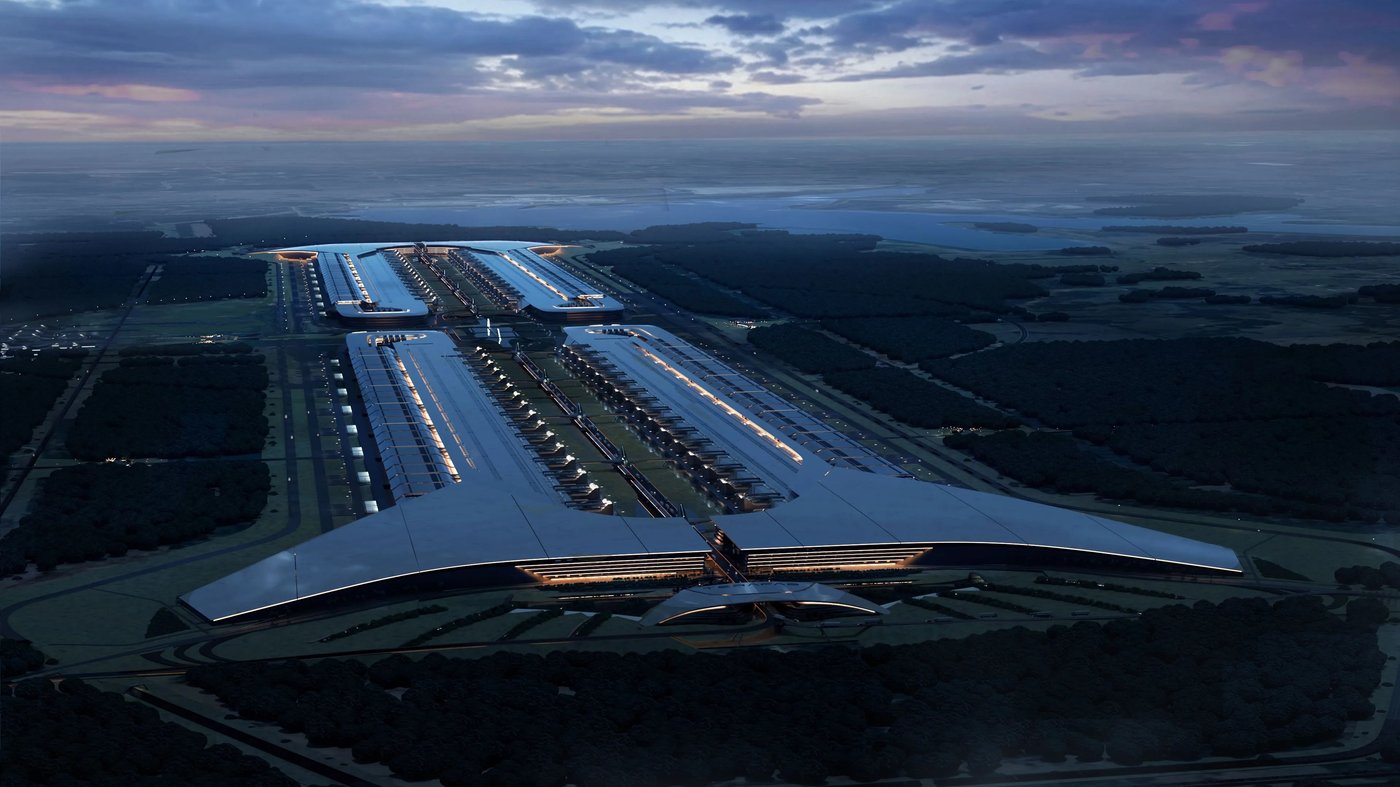
The purchasing managers began arriving in Tokyo this month, a few at a time, with the same question for the people who sell deposition chambers and etchers. If we wanted a million wafers a month, when could we have the tools? The number came from Terafab, the chip venture associated with Elon Musk, which put it to Japanese equipment makers informally this autumn, according to Nikkei. The date attached to it was after 2032.
A million wafers a month is not a target so much as a category error until you break it apart. Terafab’s plan divides roughly into 700,000 wafers of memory and more than 300,000 of logic, running simultaneously on the same site. That is about forty times the planned capacity of Rapidus at its Chitose plant in Hokkaido, the government-backed foundry that has become the reference point for ambitious Japanese semiconductor projects. The memory portion alone is close to Samsung’s entire DRAM output of 650,000 to 700,000 wafers a month.
A Number Without a Building
Nothing in the proposal describes a fab. It describes an appetite. A facility at that scale would need cleanroom space measured in hundreds of thousands of square meters, a power connection that a regional grid would have to plan around, water rights in a place that has them, and a workforce that does not currently exist in one city. Each of those takes longer to arrange than the equipment does, and the equipment is the part everyone talks about because it is the part with a lead time.
The toolmakers are the first to be asked and the last to commit. An order book is a promise made by a supplier who has to expand its own factory to keep it, and the Japanese equipment industry has spent a decade being careful about promises. A purchasing executive at one of those firms would want to know who is paying, on what schedule, and what happens to the order if the first phase slips. None of that appears in an informal conversation about a target for 2032.
The Tools Arrive Before the Concrete
There is a sequence the industry follows, and it starts with the machines. Lithography scanners, etch chambers and deposition tools are ordered years before a building is finished, because the suppliers cannot make them faster than that; the shortage of extreme-ultraviolet lithography in particular has been flagged by ASML for 2027 and 2028, and the two Korean memory makers are already competing for those slots. A new entrant asking for a million wafers a month of capacity would be asking for a share of a queue that existing customers have been standing in for years.
That is where the plan meets its first real constraint, and it is not money. Tool allocation is relational. Suppliers reserve capacity for customers with a history of paying, a known process and a roadmap they can plan against. A venture with a target and no fab competes for slots against companies that have been buying for thirty years, and it does so at the back of the line.
Who Pays for the Concrete
Musk has built capital-intensive businesses before and financed them in ways that made conventional lenders uncomfortable. A wafer fab is a harder case than a rocket factory, because the output is a commodity priced by a cycle that turns faster than the depreciation schedule. The memory half of the plan is the more exposed: DRAM margins swing, and a new entrant with no cost position and no customer relationships would be selling into a market where the incumbents set the price.
The Texas side of the story adds a political variable. The Information reported that SpaceX is building a supercomputer facility at Starbase, and that the state’s newly elected governor, Hinojosa, may let some data-center plans slip. A chip venture and a compute build-out in the same state, under the same founder, sharing the same power and permitting apparatus, would compete with each other for the scarcest input either needs.
The Record of Plans Like This
Semiconductor history is a list of capacity announcements that became something smaller. The pattern is not dishonesty so much as sequence: a target is set to attract suppliers and capital, the first phase is built, the market moves, and the remainder is re-phased. Projects that survive do so because a customer committed before the ground was broken.
That is the question the Japanese equipment makers are effectively asking, and it is the one the purchasing managers cannot answer yet. Who buys the first million wafers? If the answer is Terafab’s own compute build-out, the plan has an internal customer and a reason to exist. If the answer is the open market, the venture is proposing to enter the most competitive manufacturing business in the world at the largest scale ever attempted, with no process technology of its own and no announced partners.
The suppliers will keep talking, because a customer that might order a thousand tools is worth a meeting even if it orders ten. But the toolmakers have learned to price optimism, and the price is paid in deposits and take-or-pay terms rather than in press coverage. The purchasing managers who flew to Tokyo this month will come back with a schedule that has dates on it, and those dates will say more about the plan than the number did.